Group publishes research results in Chemical Engineering Journal

Schematic representation of SiO2@MXene and PDMS/SiO2@MXene preparation process
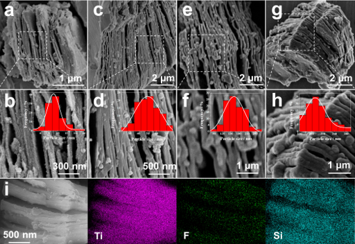
FE-SEM maps of SiO2@MXene-x (x=0.1 (a, b), 0.25, (c, d), 0.5 (e, f) and 0.75 (g, h)) and their size distributions of SiO2 particles (as inset)
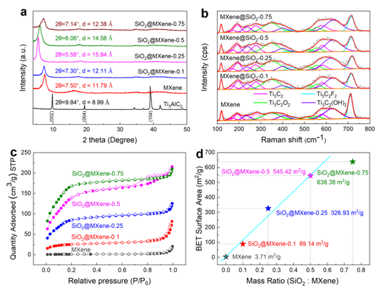
XRD (a), Raman (b), N2 adsorption/desorption isotherms (c) and plots of specific surface area versus SiO2 content for MAX, MXene and SiO2/MXene (d)
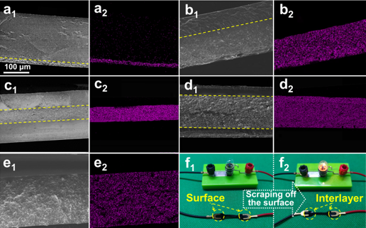
SEM maps of PDMS/MXene (a) and PDMS/SiO2@MXene (b-e) cross sections and EDS maps of Ti elements;
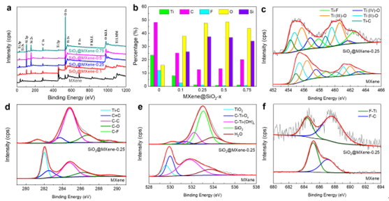
XPS maps of MXene and SiO2@MXene (a) and ratios of the content of each element (b); high-resolution XPS of MXene and Ti 2p (c), C 1s (d), O 1s (e) and F 1s (f) of SiO2@MXene-0.25
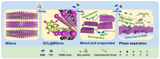
Intercalation and PDMS of SiO2 in MXene/ SiO2@Mxene-0.25 Diagram of the formation mechanism of the sandwich structure
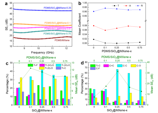
EMI SET (a) and average T, A, and R values of PDMS/SiO2/MXene in the X-band; The relationship between the Ti component content in the prepared filler and the corresponding PDMS composite membrane and the average SER (c), as well as the relationship between the C component and the average SEA (d)
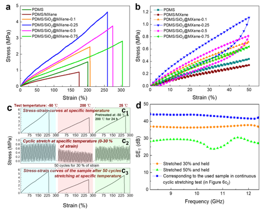
Room temperature stress-strain curves (a) and cyclic tensile curves (b) of PDMS and PDMS/SiO2/MXene films; Stability testing of mechanical properties of PDMS/SiO2/MXene-0.25 after pre-treatment under extreme conditions (extreme temperature or tension) (c); Electromagnetic interference shielding performance of PDMS/SiO2/MXene-0.25 under different states (d)
Article links:https://www.sciencedirect.com/science/article/pii/S1385894723005843